
1. Hardware Guide (LTE Extension Board)
1.1. Using mini-spacers with the main board
When the Spresense main board is used alone without the extension board, it can be convenient to install mini-spacers in the 4 corners of the main board.
The mini-spacers are fixed with screws. The mini-spacers and screws must be non metallic. The screw diameter is 2mm, and the screw length is 3mm.
They are not included in the product package of the Spresense main board, so they have to be purchased separately.
| Using metal mini-spacers and screws will have big negative effect on the reception performance of the GNSS. Make sure you use non metallic parts. |
| Vendor | Mini-spacer | Screw |
|---|---|---|
HIROSUGI |
AS-2003 |
PC-0203 |
1.2. Notes on installing and removing the Add-on board from the mainboard
Spresense allows you to install a dedicated add-on board on the main board.
When installing or removing an add-on board, be sure to install or remove it slowly in a vertical direction to the pin sockets on the Spresense mainboard.
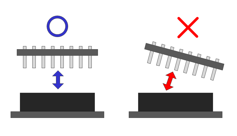
| If you remove the board in such a way that it has a rotation angle with the Spresense main board, you will not only bend the pins of the add-on board, but you will also deform or destroy the contact hardware inside the pin sockets of the Spresense main board and causing a failure. |
| The maximum pin size that can be inserted into the mainboard socket is a square pin with a side of 0.64mm. Inserting pins larger than this size or pins that have been deformed into the socket will deform or destroy the contact hardware inside the pin socket as well. This may cause a failure. |
1.3. Setting the operating voltage of the pin sockets on the LTE extension board
Spresense The I/O voltage of pin header CN9 on the LTE extension board can be switched between 5V and 3.3V by changing the jumper position on CN2. The factory default is set to 5V.
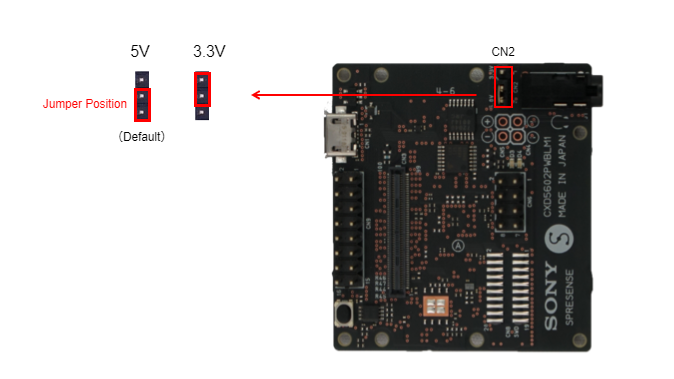
| Be sure to turn off the power of Spresense before changing the insertion position of CN2. If you change the position while the power is on, you may damage Spresense. |
| Set the voltage so that it is the same as the operating voltage of the external board, such as a sensor, connected to the LTE extension board. Incorrect setting may destroy the connected board. |
1.4. The function of the pins for external connections on the main board and LTE extension board
Spresense can be connected to external devices by connecting jumper wires to the pin sockets on the main board or LTE extension board as shown in the figure below.
The functions of each pin, along with those of other Spresense boards, are listed in the hardware design document.
Each pin of the CXD5602GG in Spresense has multiple functions.
1.4.1. For use in the Spresense Arduino environment
The main functions of the pins are "GPIO" in Mode 0 and the functions described in Mode 1.
You don’t need to be particularly aware of the pin mode when using it in the Arduino environment.
1.4.2. When using on the Spresense SDK
The CXD5602GG has pin groups, and the mode settings for each pin can be made for each pin group.
The pin groups are listed in the "Pin Group" column in the pin list.
For details on how to change the mode, refer to
It is described in the following section.
NOTE:In Spresense, there are places where the same signal line is connected to several other connectors. When using this signal, be sure to set the connection of the connector not in use to Open (or Hi-Z).
| Be sure that the voltage applied to each pin does not exceed the maximum absolute rated voltage shown in the pin list. The application of excessive voltage may cause the Spresense board to malfunction. |
1.5. Power supply when connecting an external device to the Spresense board
The power supply system diagram when the Spresense main board and LTE extension board are combined is shown below.

When connecting an external device to Spresense and supplying power from the pins for power supply of Spresense, do not exceed the maximum output current value shown in the figure.
When LTE communication is used, the LTE module alone consumes a maximum of 1.2A of current. Connect the power supply so that the total current that can be supplied from the microUSB of the main board and LTE extension board is about 1.5A. For reliable LTE communication, make sure that more than 1.5A can be supplied from the microUSB of the Spresense LTE extension board.
1.6. Spresense Power and reset timing sequence during boot
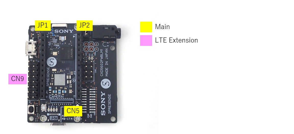
SpresenseThe following figure shows the sequence chart for each power supply and reset from the time the main board and LTE extension board are combined and power is supplied from the microUSB pin until CXD5602 starts up. The sequence chart for each power supply and reset is shown in the figure below.
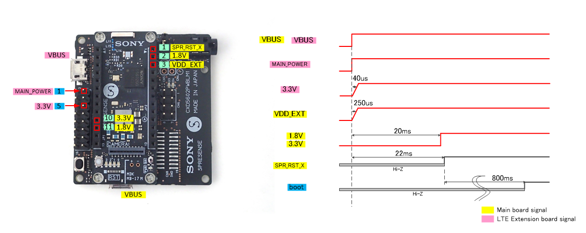
The "boot" in the figure shows the time it takes for one GPIO pin of CXD5602 to be set to High and output immediately after booting in the Arduino IDE and Spresense SDK.
1.7. How to use the reset function
Spresense can be used to reset the system in the following ways.
-
Press SW2 on the main board
-
UART connection by serial monitor, etc. (DTR signal trigger)
When the system is reset, the power supply will be stopped for a moment from CXD5247 of the LSI that manages the power supply and each power supply LSI.
The reset signal (XRST_PIN_1.8V) on pin 1 of JP2 on the main board outputs the system reset status. It is Low when the system reset is applied, and High (1.8V) when it is not. The signal outputs Low when the system reset is on, and High (1.8V) in other states. By using this signal, it is possible to reset the Add-on board at the same timing as the sensing processor CXD5602.
1.8. About the I/O current value of CXD5602
Since the CXD5602 is a very low-power processor, the maximum I/O port current is about 6mA.
1.9. How to use I2C
In Spresense, the main board and the LTE extension board each have one pin that can be used for I2C connections (the LTE extension board is used exclusively with PWM2 and PWM3).
The interface voltage is 1.8V for the main board and 5V or 3.3V for the LTE extension board.
The maximum communication speed is 400kbps.
The I2C of the main board and the LTE extension board are separate systems.
The main board I2C (I2C0) is pulled up to 1.8V at 4.7kΩ, and the LTE extension board I2C (I2C1) is pulled up to 5V or 3.3V at 1KΩ via the level shifter on the board.
1.10. How to use UART
When using the LTE extension board in Spresense, one terminal is provided on the main board that can be used for UART connection with flow control.
The interface voltage is 1.8V and the maximum communication speed is 1.8432Mbps.
1.11. How to use SPI
In Spresense, the main board and LTE extension board each have one pin that can be used for SPI connection.
SPI on both boards can only be used in master mode.
The interface voltage is 1.8V for the main board and 5V or 3.3V for the LTE extension board.
Communication speed is up to 13Mbps for the main board and up to 6.5Mbps for the LTE extension board.
The main board and LTE extension board use different SPI systems, so they can be used simultaneously.
1.12. How to use PWM
Spresense provides four pins on the LTE extension board that can be used for PWM output (two of them are used exclusively with I2C).
The interface voltage is either 5V or 3.3V. The maximum frequency is 6.5MHz and the maximum resolution is 15 bits.
1.13. How to use SDIO
CXD5602 has a 1.8V 4-bit (or 1-bit) SD mode compatible interface that conforms to the SDIO standard, and Spresense uses a level shifter on the LTE extension board to convert the voltage to 3.3V so that microSD cards can be used.
The maximum data transfer rate for SDIO on Spresense is 21MB/s.
1.14. Precautions for using digital signals (UART/SPI/PWM/GPIO) on the LTE extension board
The Spresense uses a level shifter for the digital pin input/output of the LTE extension board to automatically switch the direction and perform voltage conversion. Please see the schematic below.
This level shifter is always pulled up to 5V or 3.3V with 1kΩ on the pin socket side.
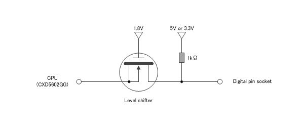
If the circuit to be connected to the pin socket is a low impedance circuit, the threshold to be detected by the CPU will fluctuate. This will cause problems with interpreting the signal.
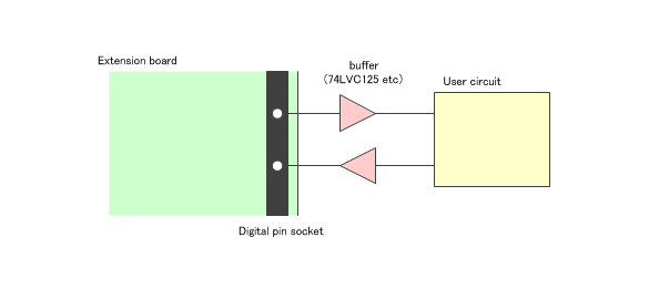
In that case, for signals whose input/output direction does not change, it is a good idea to insert a one-way buffer between the pin socket and the connected circuit as shown in the figure below.
1.15. How to use the A/D converter
Spresense has two A/D converters (ADCs) on the main board (SEN_AIN4 and SEN_AIN5) and two on the LTE extension board (SEN_AIN0 and SEN_AIN1).
Compared to the LPADC (Low Power ADC) pins SEN_AIN4 and SEN_AIN5, the HPADC (High Performance ADC) pins SEN_AIN0 and SEN_AIN1 provide high speed A/D conversion. When A/D converting DC voltage such as power supply voltage and temperature data, it is recommended to use LPADC which can A/D convert from 0V using full range.
The table below shows the specifications of each ADC pin.
| Analog pin number | CXD5602 pin name | Type | Main board input voltage (V) | LTE extension board input voltage (V) |
|---|---|---|---|---|
A2 |
SEN_AIN4 |
LPADC |
0 - 0.7 |
- |
A3 |
SEN_AIN5 |
LPADC |
0 - 0.7 |
- |
A4 |
SEN_AIN0 |
HPADC |
- |
0 - 5.0 |
A5 |
SEN_AIN1 |
HPADC |
- |
0 - 5.0 |
Note the mapping between the CXD5602 pin (name on the schematic) and the analog pin number, and the input voltage ranges to the boards.
On the LTE extension board, voltage dividers convert the input signals before they are input into the CXD5602 ADC pins. When 5.0V is applied to the analog pins of the LTE extension board, the HPADCs of SEN_AIN0 and SEN_AIN1 are reduced to 1.4V by the circuit shown below.
The ADC reference voltage uses 0.7V generated by CXD5247 on the main board.
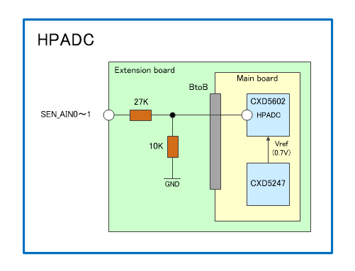
When connecting a circuit with impedance to the CXD5247 ADC pins, e.g. when checking the operation of the ADC by varying the applied voltage via a variable resistor, the value of the variable resistor and the resistance of the voltage divider circuit above determine the input voltage to the ADC pins.
1.15.1. When used in the Spresense Arduino environment
The A/D converter output is given as unsigned 10-bit data.
The sampling frequency is set to be 64Hz for LPADC and 16KHz for HPADC.
1.15.2. When used on the Spresense SDK
The A/D converter output is given as signed 16-bit data. Both LPADC and HPADC convert 10-bit raw data to signed 16-bit data and output it, and the output value range is -32768 (= 0x8000) to 32704 (= 0x7fc0).
For an example of how to use the ADCs, please see the Spresense SDK tutorial.
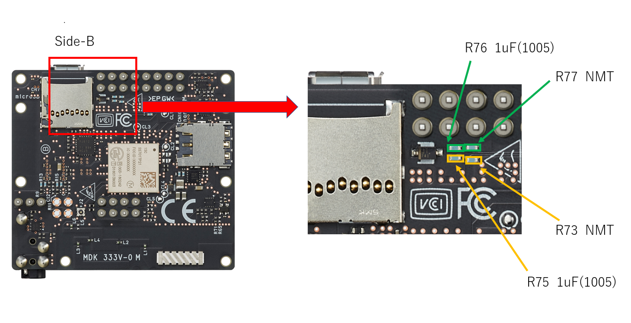
1.15.3. A/D conversion of signals with low values
In order to change the gain with HPADC and A/D convert for a smaller signal such as voice or various sensors, it is recommended to cut the input signal to the HPADC port with DC cut as shown in the figure below. By cutting DC, the analog port on the extension board and the peak-peak voltage input to the CXD5602 pin become equal.
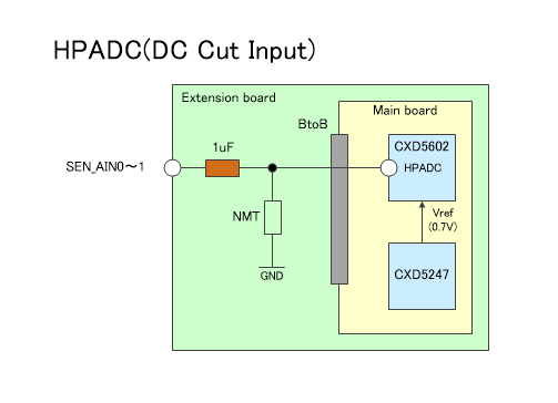
To use this function with the LTE extension board, soldering on the LTE extension board as shown in the figure below is required. This work involves soldering of small components and modification of the board. Please note that this should only be attempted by people with the appropriate skills and equipment.
| Soldering operations described here are not covered by the product warranty under any circumstances. You do so at your own risk. |
1.16. Powering the main board with external power
The maximum current that can be drained from the Spresense main board micro USB connector is 500mA. This is true also when both the main board and extension board are mounted and have separate USB power connected. The 500mA current that is sourced by the main board will be shared with the Add-on board too.
In case that the 500mA current from the micro USB connector is not sufficient it is possible to supply more power using the battery terminal CN1 on the main board. The CN1 battery connector’s recommended operating voltage is 3.6 to 4.4V with an absolute maximum voltage of 5.5V. Using the CN1 battery connector the sourced current from EXT_VDD (JP2 pin number 3) to an Add-on board can be increased.
See the table below for recommended battery connector that will fit CN1.
It is necessary to solder on the main board to mount a battery connector on CN1.
| Modifying the Spresense boards will void the warranty. Please do it at your own risk. |
| Vendor | Type | Comment |
|---|---|---|
Japan Crimp Terminal Mfg. Co., Ltd. |
S2B-PH-K-S |
PH male connector |
PHR-2 |
PH female connector |
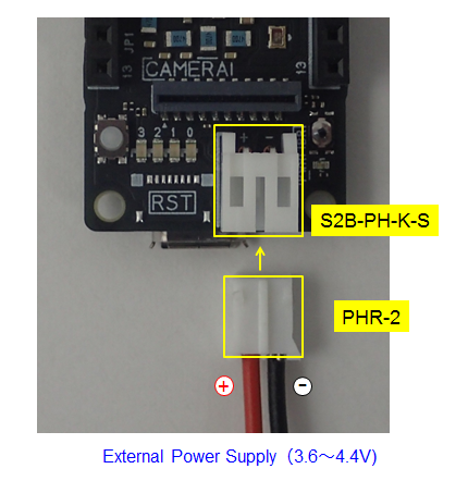
Powering the main board via the CN1 battery connector will boot the Spresense system even if the micro USB is not connected.
| Do not use the microUSB connector on the main board and extension board when power is supplied from the PH connector (CN1) on the main board. Also, disconnect the external power supply when debugging. |
1.17. Microphone Usage
Spresense supports connecting up to two analog microphone or up to four digital microphones via the 2.54mm pitch pin header mounted on the LTE extension board.
The factory default setting is for analog microphones. To use digital microphones, some reconfiguration of the LTE extension board is required. This involves soldering of small components and modification of the board and should only be performed by a person with the appropriate skills and equipment.
| Soldering operations described here are not covered by the product warranty under any circumstances. You do so at your own risk. |
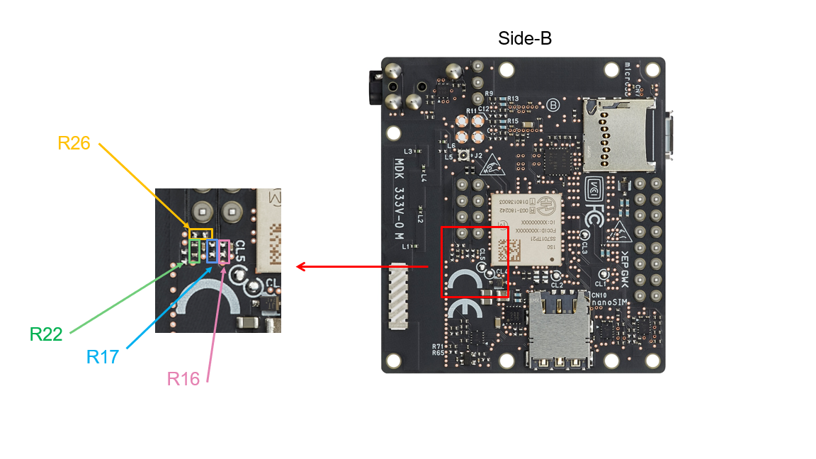
1.17.1. Microphone channel placement
The following figure shows the arrangement of the microphone channels on the LTE extension board.
A and B represent the analog microphone channels, and D01 and D23 in the same color represent the corresponding digital microphone channels.
If the input settings for analog or digital microphones are set separately for each channel, sufficient input sound quality performance may not be obtained. It is recommended that all channels are set to either analog or digital microphone input.

1.17.2. How to switch from an analog microphone to a digital microphone input
To switch from analog to a digital microphone input, the following two steps are required:
-
Remove R22 and mount 0Ω to R26 (or short-circuit with a jumper wire etc.)
-
Mount 0Ω to R16 (D01 channel) and R17 (D23 channel) (or short-circuit with a jumper wire etc.)
1.17.3. How to connect an analog microphone
1.17.3.1. Dynamic microphone
The microphone connection pin header on CN6 has two analog microphone input terminals (MICA and MICB). These pins are AC-coupled by capacitors. When using analog microphones, please use the GND of CN6 as the microphone GND to minimize noise.
1.17.3.2. Electret microphone
Spresense allows connection of a capacitor-based 2-wire electret microphone with a reference voltage of 2.0V. A bias voltage of 2.0V is applied to the microphone input terminal of the CN6 pin header with a load resistance of 2.2kΩ.
Examples of electret microphones that can be used are shown below. The recommended value of the load resistance for the following microphones is 2.2kΩ.
| Manufacturer | Product Name |
|---|---|
CUI |
CMC-5044PF-A |
PUI |
POM-3535P-3-R |
Soberton |
EM-6022P |
1.17.3.3. Analog MEMS Microphone
When connecting an analog MEMS microphone, connect the microphone bias terminal of the CN6 pin header to the power supply pin of the microphone. The bias pin supplies the microphone with a 2.0V voltage.
The following are examples of analog MEMS microphones that can be used:
| Manufacturer | Product Name |
|---|---|
Knowles |
SPU0414HR5H-SB |
Knowles |
SPH1642HT5H-1 |
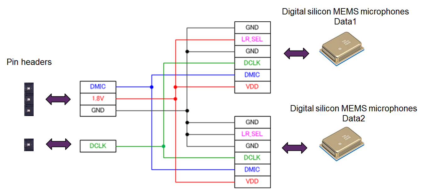
1.17.4. How to connect a digital microphone
The recommended method for connecting digital microphones is shown below. It is possible to connect two digital silicon MEMS microphones by setting the polarity of the left/right switching signal (LR_SEL) of one digital microphone to LOW and the other to HIGH to combine the 3 pins (DMIC, DCLK, GND) for each microphone channel and the 1.8V power supply. The 1.8V power supply can be supplied from the MIC_BIAS pins of the A and B channels, so please use them separately.
The following are examples of digital silicon MEMS microphones that can be used.
| Manufacturer | Product Name |
|---|---|
Knowles |
SPH0641LU4H-1 |
Knowles |
SPM0423HD4H-WB |
Infineon |
IM69D130 |
1.18. How to use the speaker
Spresense has a stereo class-D output amplifier in CXD5247 mounted on the main board, which can be used to drive two speakers. However, the main board by itself does not supply 3.3V power to the Class-D amplifier of CXD5247, so the speakers cannot be used.
In order to use the speakers, you need to supply a low-noise 3.3V power supply to pins 1 and 3 of the board-to-board connector CN4 on the main board. Supply sufficient current value according to the speaker you are using.
This 3.3V power supply is designed to be supplied when used with the LTE extension board.
The mainboard is factory configured to match the headphone output of the LTE extension board. In order to use the speaker, you need to replace the chip components on the mainboard and solder them to the LTE extension board. This work involves soldering small components and modifying the board, so please make sure you have the proper skills and equipment to do this.
| If you perform any of the soldering operations described here, the product warranty will not apply under any circumstances. Please perform this work at your own risk. |
1.18.1. Working on the main board
Replace the component that smoothes the Class-D output of CXD5602 according to the following instructions.
-
R15, 16, 17, 18 → 15uH/220mA(2012) [Parts with the orange frame in the figure below]
Change to inductor
Taiyo Yuden BRL2012T150M is recommended. -
C45, 46, 47, 48 → 0.47uF(1005) [Parts with the green frame in the figure below]
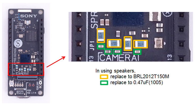
| If you make this change, do not use the headphone output of the LTE extension board. |
1.18.2. Working on the LTE extension board
Solder a 2.54mm pitch pin header for the speaker connection to CN4 and CN5 (or solder the speaker cord directly).
| The Spresense board is designed to run the left and right speakers independently. Be careful not to connect the left and right negative sides together. |

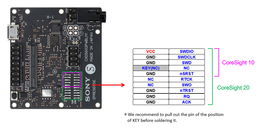
1.19. How to use the JTAG debugger
The Cortex-M series SWD-compatible JTAG debugger can be used with Spresense by connecting it to the CoreSight 10 or 20 connector.
In order to use this function, soldering work to the extension board is required. This involves soldering small components and modifying the board, so please be aware that this should only be done by people with the appropriate skills and equipment.
| If you perform any of the soldering operations described here, the product warranty will not apply under any circumstances. Please perform this work at your own risk. |
Solder the pin header for CoreSight 10 or 20 to CN8 on the extension board.
Depending on the CoreSight cable to be used, the hole for the KEY may be filled. Before soldering, pull out the pins that correspond to the KEY shown in the figure below using radio pliers or the like.
The following are examples of pin headers that can be used.
| Manufacturer | Pin header (10 poles) | Pin header (20 poles) |
|---|---|---|
Hirosugi-Keiki |
PSM-720153-05 |
PSM-720153-10 |
Samtec |
FTS-105-01-L-DV-TR |
FTS-110-01-L-DV-TR |
HARWIN |
M50-3600542 |
M50-3601042 |
Jc Electronics Co. |
IKHSM28-D10G-H1.5 |
IKHSM28-D20G-H1.5 |
1.20. How to use GNSS
1.20.1. About On-board chip antenna for GNSS
The Spresense is equipped with a chip antenna for GNSS on the main board, and positioning is possible in that state.
The characteristics of the onboard antenna are shown below. The characteristics of on board GNSS chip antenna (pdf)
1.20.2. How to use the external antenna for GNSS
The Spresense can also be used to connect an external uFL connection type antenna to the main board for higher performance positioning.
If you connect an external antenna to the uFL connector, higher-performance positional measurement is possible. To do this you have to solder a uFL connector on the main board. This modification requires soldering of very small components and should only be attempted by people with appropriate skills and equipment.
| Modifying the Spresense hardware by performing soldering work as described here will void the product warranty. Please proceed at your own risk. |
The following steps will describe the necessary work needed to fit an uFL connector to be able to use an external GNSS antenna.
-
Mount the uFL connector on CN3, see the picture below.
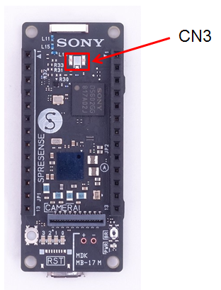
| Vendor | Model |
|---|---|
Hirose Electric |
U.FL-R-SMT-1 |
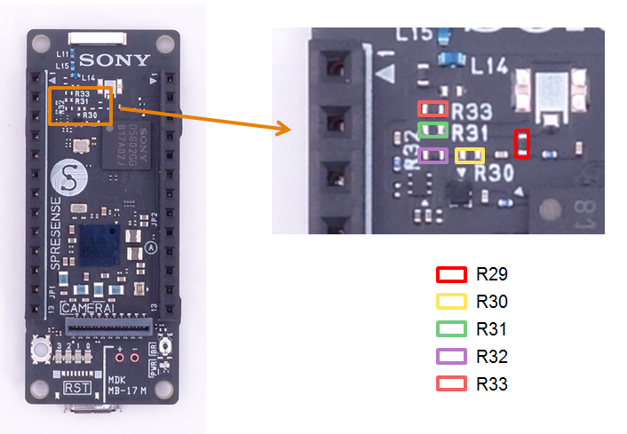
-
Depending on the type of the antenna you plan to use, the resistor chips have to be changed on the main board as shown in the table below.
In the table below, "OPEN" stands for the status that a part is not mounted in the applicable location, and "CLOSE" stands for the status that it is short-circuited with 0 Ω resister or a wire.
| Antenna | R29 | R31 | R33 | R30 | R32 | Note |
|---|---|---|---|---|---|---|
chip (on board) |
CLOSE |
OPEN |
CLOSE |
OPEN |
CLOSE |
default |
passive (external) |
OPEN |
CLOSE |
OPEN |
OPEN |
CLOSE |
|
active (external) |
CLOSE |
OPEN |
CLOSE |
CLOSE |
OPEN |
3.3V supplied to antenna |
1.21. Spresense Add-on board / extension board / case design
1.21.1. Spresense HW design material
Spresense publishes various hardware design materials for all boards that are useful for designing Add-on boards, extension boards, and cases.
-
Schematics
-
Bill of Materials
-
Dimensions
-
Parts layout
-
2D CAD DATA(DXF)
-
3D CAD DATA(STEP)
In addition, the connector pin list and GNSS onboard chip antenna characteristics are also disclosed.
These are collectively published in Hardware Design Documents.
1.21.2. Precautions for board dimensions when designing Spresense Add-on boards
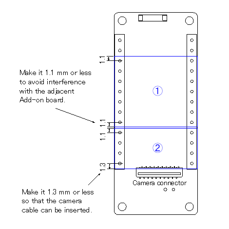
In order to mount multiple Spresense Add-on boards in the pin sockets on the main board, it is necessary to pay attention to the board dimensions.
The figure below shows the points to be noted when designing the board dimensions, taking as an example the case of designing two Add-on boards (1) and (2).
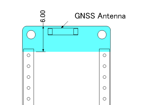
1.21.3. Precautions when using the onboard chip antenna for GNSS on the Spresense main board
When positioning GNSS using a newly designed board and the onboard chip antenna for GNSS on the Spresense main board, pay attention to the design around the antenna in order to ensure the reception sensitivity of the antenna. .
When designing an Add-on board or extension board that overlaps the light blue colored part in the figure below, do not place metal-containing parts or copper foil patterns on the corresponding part of each board.
1.22. Countermeasures when LTE radio waves affect the cables of externally connected devices
When using an external connection device or board connected to the pin socket of the Spresense main board or the pin header of the Spresense LTE extension board at the same time, if the LTE antenna and their connection cables are close to each other, that LTE radio waves may affect the cable and cause instability.
In such cases, using a shielded cable as the connecting cable may improve the situation. In some cases, simply wrapping household aluminum foil around the cable may help.
The connection cable that comes with the Spresense camera board is a shielded cable, but if the operation is still unstable even if you use such a shielded cable, wrapping the cable with the shield sheet below will improve the situation.
| Vendor | Shield sheet |
|---|---|
KEMET |
EFG2(03)-240X240T0800 |