
1. How-to Guides
1.1. Using mini-spacers with the main board
When the Spresense main board is used alone without the extension board, it can be convenient to install mini-spacers in the 4 corners of the main board.
The mini-spacers are fixed with screws. The mini-spacers and screws must be non metallic. The screw diameter is 2mm, and the screw length is 3mm.
They are not included in the product package of the Spresense main board, so they have to be purchased separately.
| Using metal mini-spacers and screws will have big negative effect on the reception performance of the GNSS. Make sure you use non metallic parts. |
| Vendor | Mini-spacer | Screw |
|---|---|---|
HIROSUGI |
AS-2003 |
PC-0203 |
1.2. Precautions when installing/removing the Add-on board on the main board and the Arduino shield on the extension board
Spresense can be equipped with a dedicated Add-on board for the main board and a commercially available Arduino shield for the extension board.
When installing or removing these boards, be sure to slowly insert or remove them vertically to the pin sockets of each Spresense board.
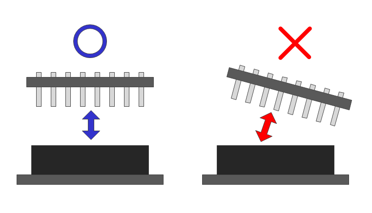
| If you remove each Spresense board so that it has a rotation angle, it will not only bend the pins of the Add-on board and extension board, but also deform the contact metal fitting inside the pin socket of the Spresense board. It may damage the Spresense board. |
| The maximum pin that can be inserted into the socket of each Spresense board is a square pin with a side of 0.64 mm. Inserting a pin with a size larger than this size or a deformed pin into the socket will similarly deform or destroy the contact metal fitting inside the pin socket, resulting in a failure. |
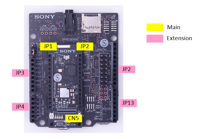
1.3. Setting the operating voltage of the GPIO pin sockets on the extension board
The operating voltage on pin socket JP2 and JP13 of the extension board can be set to 5V or 3.3V by changing the position of the jumper on JP1.
The extension board operating voltage is set to 5V when shipped.

|
WARNING
|
| Socket | Pin | Name |
|---|---|---|
JP3 |
2 |
IOREF |
JP2 |
3 |
AREF |
1.4. Function of the external connection pin of the main board and extension board
Spresense can connected to an external device by connecting a jumper wire to the pin socket on the main board or extension board as shown in the figure below.
The functions of each pin are listed together with other Spresense board pins in the hardware design materials.
Each pin of CXD5602GG installed in Spresense has multiple functions.
1.4.1. When using in Spresense Arduino environment
As for the function of the pin, it is possible to mainly use the function described in "GPIO" of mode 0 and mode 1.
You don’t need to be aware of the pin mode when using it in an Arduino environment.
1.4.2. When used on the Spresense SDK
The CXD5602GG has pin groups, and the mode setting for each pin can be set for each pin group.
Pin groups are listed in the "Pin group" column of the pin list.
How to change the mode is described below.
| In Spresense, there are places where the same signal line is connected to multiple different connectors. When using this signal, make sure to open (or Hi-Z) the connection of the connector that is not used. |
| Make sure that the voltage applied to each pin does not exceed the maximum absolute rated voltage listed on the pin list. Applying an overvoltage may cause the Spresense board to malfunction. |
1.5. Regarding power supply when connecting externally connected devices to the Spresense board
The Spresense power system diagram when the main board and extension board are combined is shown below.
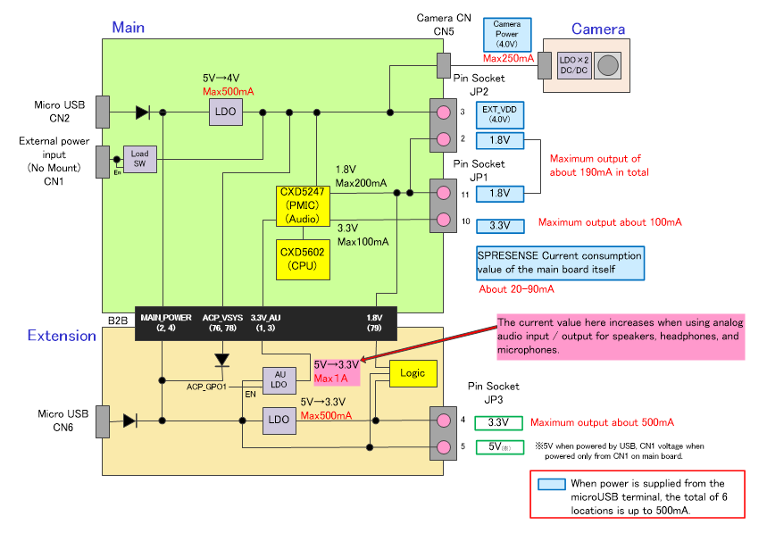
When connecting an external device to Spresense and supplying power from the power supply pin of Spresense, do not exceed the maximum output current value shown in the figure.
1.6. Spresense Power and reset boot timing sequence
The figure below shows the sequence chart of each power supply and reset from the time the Spresense main board and extension board are combined and the power is supplied from the microUSB terminal until CXD5602 starts up.
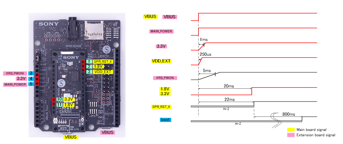
"Boot" in the figure shows the time until one GPIO pin of CXD5602 is set to High and output immediately after booting on the Arduino IDE and Spresense SDK.
1.7. How to use reset function
Spresense can reset the system in the following way.
-
Press SW2 on the main board.
-
UART connection (DTR signal trigger) by serial monitor etc.
-
Reduce the signal level of JP3’s 3rd pin of the extension board to Low (see details below)
When a system reset is applied, from the CXD5247 of the LSI that manages the power supply and each power supply LSI Since power supply stops for a moment, caution is required when connecting an external circuit to an extension board or Add-on board.
Resetting pin No.3 of JP3 on the extension board can be used as bidirectional. That is
-
Input the signal to reset the system from the extension board.
-
Reset the system connected outside the extension board.
Although it can be used as any of the above, please connect the recommended circuit shown below as an external circuit. However, as a user device to be connected, a microprocessor LSI We assume high impedance devices such as.
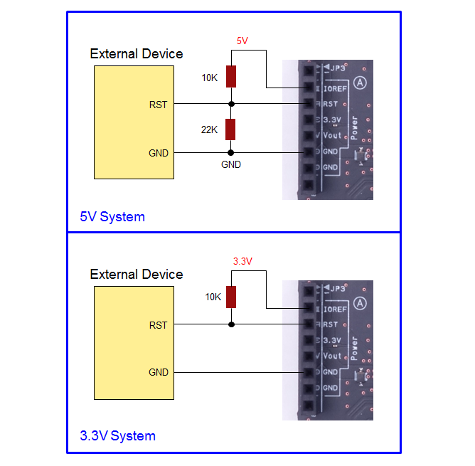
Also, the reset signal (XRST_PIN_1.8V) on pin No.1 of JP2 on the main board outputs the system reset status. It is Low when the system reset is applied, and in other states It outputs High (1.8V). By using this signal, it is possible to reset the Add-on board etc at the same timing as the sensing processor CXD5602.
1.8. CXD5602 I/O current
CXD5602 is a very low power processor. Typical I/O current values are limited to around 6mA.
1.9. How to use the I2C
Both Spresense main board and extension board have I2C terminals. The interface voltage is 1.8V on the main board, and 5V or 3.3V on the extension board.
How to set the interface voltage on the extension board is described in this chapter.
The main board and extension board use the same system for I2C. They can be connected to several I2C slave devices at the same time if the slave devices have different slave addresses.
| Board | Voltage | Max clock speed | Pull up | Comment |
|---|---|---|---|---|
Main |
1.8V |
1MHz |
4.7kΩ |
Additional bus exposed on the B2B connector |
Extension |
5V or 3.3V |
1MHz |
1kΩ |
Voltage selectable via jumper |
Read Spresense Hardware Documents for more details.
Refer the Wire Library for more information on how to use the I2C from the Arduino environment.
1.10. How to use the UART
The Spresense main board and extension board have UART terminals.
It is not possible to use the UART on both the main board and the extension board at the same time.
The extension board is configured to have the UART enabled when it is shipped. To use the UART pins on the main board when attached to the extension board, a 2.54mm pitch jumper have to be connected to pin 1 and 2 on JP10 of the extension board to disable the extension board UART. No jumper is supplied with the Spresense boards so this has to be purchased separately.
When the extension board UART is activated, the UART pins (D00, D01, D27 and D28) of the main board cannot be used as GPIO.
| Board | Voltage | Max transmission rate | Comment |
|---|---|---|---|
Main |
1.8V |
1.8432Mbps |
Flow control available on pin socket and B2B connector. |
Extension |
5V or 3.3V |
1.8432Mbps |
Can be disabled via jumper. Initial setting when shipped: On. |
The B2B connector has all the UART related signals (including handshake signals UART2_CTS and UART2_RTS) that can be used on custom boards. Refer to Spresense Hardware Documents for details.
1.11. How to use the SPI
Both the Spresense main board and the extension board have SPI terminals. SPI can only be used in master mode on both boards.
You can use both SPI functions on main board and extension board at the same time because the boards do not share the same bus.
| Board | Voltage | Mode | Max speed | Comment |
|---|---|---|---|---|
Main |
1.8V |
Master only |
13Mbps |
SPI5 |
Extension |
5V or 3.3V |
Master only |
39Mbps (Tx only) |
SPI4 |
Read the SPI Library documentation for more information on how to use the SPI from the Arduino environment.
The max speed stated in the table above is the rated speed for the CXD5602. When used together with the voltage level shifters on the extension board the max speed drops to around 20MHz. This speed is also influenced of the environment.
1.12. How to use the PWM
| Board | Voltage | Resolution | Max frequency | Comment |
|---|---|---|---|---|
Main |
1.8V |
15bit |
6.5MHz |
PWM0, PWM1, PWM2 and PWM3 but only available through B2B connector. |
Extension |
5V or 3.3V |
15bit |
6.5MHz |
PWM0, PWM1, PWM2 and PWM3 |
Read Spresense Hardware Documents for details about the PWM on the main board B2B connector.
1.13. How to use the SDIO
The CXD5602 has a 1.8V 4-bit (or 1-bit) SD mode interface compliant with the SDIO standard, and Spresense can use the microSD card by converting the voltage to 3.3V using a level shifter on the extension board .
The maximum data transfer rate for Spresense’s SDIO is 21 MB/s.
1.14. Attention when using digital signals (UART/SPI/PWM /GPIO) on extension board
It is possible to change voltage and direction of a signal for a digital pin input and output automatically on the extension board by connecting a circuit with the following characteristics.
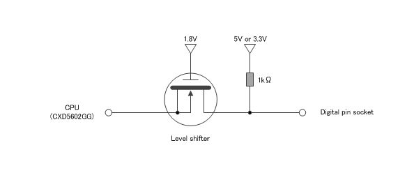
The pins of this voltage level transfer device at socket side is always pull to 5V or 3.3V by 1kΩ resistor.
If a circuit with low impedance is connected to the pin socket, CXD5602 will not be able to detect the threshold voltage which will result in incorrect detection of the logic value.
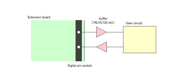
In this case, it is recommended to insert a one-way buffer, as shown in the diagram, for the signal where the input/output direction does not change between the pin socket.
1.15. How to use the A/D converter
Spresense has 2 systems (SEN_AIN4, SEN_AIN5) on the main board and 6 systems (SEN_AIN0 to SEN_AIN5) A/D converter (ADC) on the extension board. Pins SEN_AIN4 and SEN_AIN5 on the main board are used exclusively with the same signal pin on the extension board.
Compared to LPADC (Low Power ADC) of SEN_AIN2 to SEN_AIN5, HPADC (High Performance ADC) of SEN_AIN0 and SEN_AIN1 are pins that can perform A/D conversion at high speed. When A/D converting DC voltage such as power supply voltage and temperature data, it is recommended to use LPADC which can A/D convert from 0V using full range.
The table below shows the specifications of each ADC pin.
| Analog pin number | CXD5602 pin name | type | Main board input voltage(V) | extension board input voltage(V) |
|---|---|---|---|---|
A0 |
SEN_AIN2 |
LPADC |
- |
0 - 5.0 |
A1 |
SEN_AIN3 |
LPADC |
- |
0 - 5.0 |
A2 |
SEN_AIN4 |
LPADC |
0 - 0.7 |
0 - 5.0 |
A3 |
SEN_AIN5 |
LPADC |
0 - 0.7 |
0 - 5.0 |
A4 |
SEN_AIN0 |
HPADC |
- |
0 - 5.0 |
A5 |
SEN_AIN1 |
HPADC |
- |
0 - 5.0 |
Note the pin (name on the schematic) of CXD5602 to the analog pin number and the input voltage range to the main board.
On the extension board, the voltage is converted into the A/D conversion pin of CXD5602 by resistor divider.
When 5.0V is applied to the analog pin of the extension board, LPADC of SEN_AIN2 to SEN_AIN5 is reduced to 0.7V and HPADC of SEN_AIN0 and SEN_AIN1 is reduced to 1.4V by the circuit shown below.
The reference voltage of ADC uses 0.7V generated by CXD5247 on the main board.
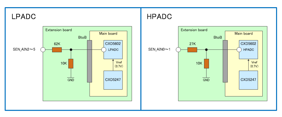
When connecting a circuit with impedance to the ADC pin, for example, when changing the applied voltage through the variable resistor to check the ADC operation, the voltage determines to the ADC pin of CXD5247 by the resistance value of the variable resistor and the resistance of the voltage divider circuit.
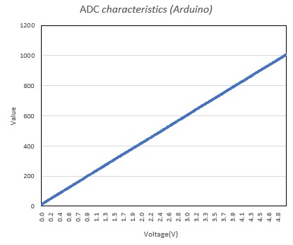
1.15.1. When using in Spresense Arduino environment
The A/D conversion value is output as unsigned 10-bit data.
The sampling frequency is set to 64Hz for LPADC and 16KHz for HPADC.
All ADCs have the following characteristics when using the Spresense extension board and input from the analog input pin of the extension board (HP ADC gain is set to -6dB).
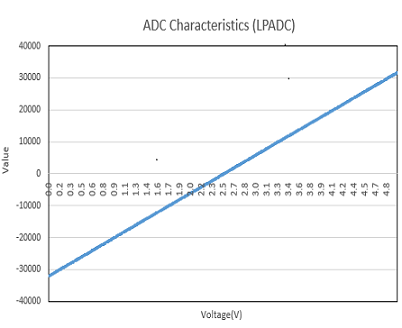
1.15.2. When using on Spresense SDK
The A/D conversion value is output as signed 16-bit data. Both LPADC and HPADC convert 10-bit raw data to signed 16-bit data and output it, and the output value range is -32768 (= 0x8000) to 32704 (= 0x7fc0).
The LPADCs of SEN_AIN2 to SEN_AIN5 have the following characteristics.
In Spresense SDK, gain and conversion speed can be changed for SEN_AIN0 and SEN_AIN1 HPADC.
Instructions for using the ADC can be found here in the Spresense SDK tutorial.
The graph of the conversion value when the gain of HP ADC is changed on the extension board is shown below.
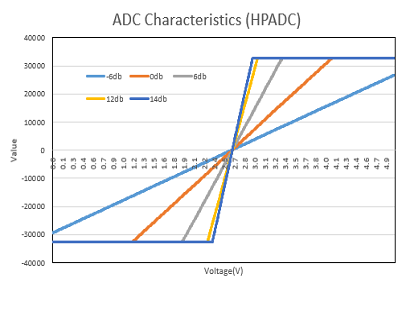
The relationship between the input voltage value to the HP ADC port of CXD5602 and the setting value of gain is described in "2.21.9 Gain Control" of CXD5602 User Manual (Posted in the table below).
The converted value is saturated in the range that exceeds the input voltage value.
| gain(dB) | Effective peak-to-peak voltage (V) on the CXD5602 pin |
|---|---|
-6 |
1.6 |
0 |
0.8 |
6 |
0.4 |
12 |
0.2 |
14 |
0.16 |
1.15.3. For A/D conversion of smaller signals
In order to change the gain with HPADC and A/D convert for a smaller signal such as voice or various sensors, it is recommended to cut the input signal to the HPADC port with DC cut as shown in the figure below. By cutting DC, the analog port on the extension board and the peak-peak voltage input to the CXD5602 pin become equal.
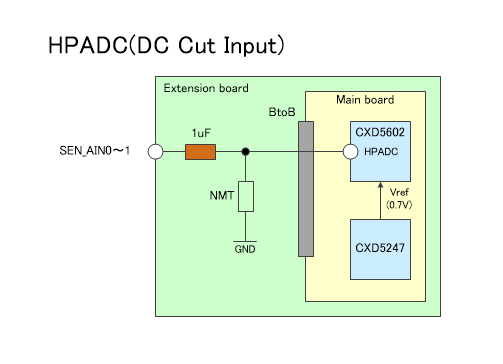
To use this function with an extension board, you need to solder it to the extension board as shown in the figure below. The work here involves soldering small parts and modifying the board. Please note that this should only be carried out by those who have the appropriate skills and equipment.
| Modifying the Spresense hardware by performing soldering work as described here will void the product warranty. Please proceed at your own risk. |
1.16. Powering the main board with external power
The maximum current that can be drained from the Spresense main board micro USB connector is 500mA. This is true also when both the main board and extension board are mounted and have separate USB power connected. The 500mA current that is sourced by the main board will be shared with the Add-on board too.
In case that the 500mA current from the micro USB connector is not sufficient it is possible to supply more power using the battery terminal CN1 on the main board. The CN1 battery connector’s recommended operating voltage is 3.6 to 4.4V with an absolute maximum voltage of 5.5V. Using the CN1 battery connector the sourced current from EXT_VDD (JP2 pin number 3) to an Add-on board can be increased.
See the table below for recommended battery connector that will fit CN1.
It is necessary to solder on the main board to mount a battery connector on CN1.
| Modifying the Spresense boards will void the warranty. Please do it at your own risk. |
| Vendor | Type | Comment |
|---|---|---|
Japan Crimp Terminal Mfg. Co., Ltd. |
S2B-PH-K-S |
PH male connector |
PHR-2 |
PH female connector |
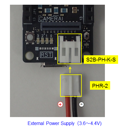
Powering the main board via the CN1 battery connector will boot the Spresense system even if the micro USB is not connected.
| Do not use the microUSB connector on the main board and extension board when power is supplied from the PH connector (CN1) on the main board. Also, disconnect the external power supply when debugging. |
| MODIFYING THE Spresense BOARD WILL VOID THE WARRANTY. PROCEED ON YOUR OWN RISK! |
1.17. How to achieve 6µA current consumption on Mainboard
It is possible to reach as low as just above 6µA during Deep Sleep using the Spresense mainboard. To achieve this the mainboard needs to be modified.
The components that needs to be removed are very small and delicate. A professional soldering iron with a very fine tip as well as a microscope is required. It is not advised to proceed if you are not fully aware of how the following changes affects the board. Some of the components are mounted due to safety reasons and these functions will be disabled after the modification.
1.17.1. Instructions
| MODIFYING THE Spresense BOARD WILL VOID THE WARRANTY. PROCEED ON YOUR OWN RISK! |
-
Remove resistor R21 to disable the POWER LED
-
Remove diode D1 for 5V_BUS.
-
Remove load switch IC8 (TCK112G) and then short pads A1,A2, B1 and B2.
-
Remove resistor R28 (XRS_PWON).
-
Remove capacitor C76 (UART_DTR).
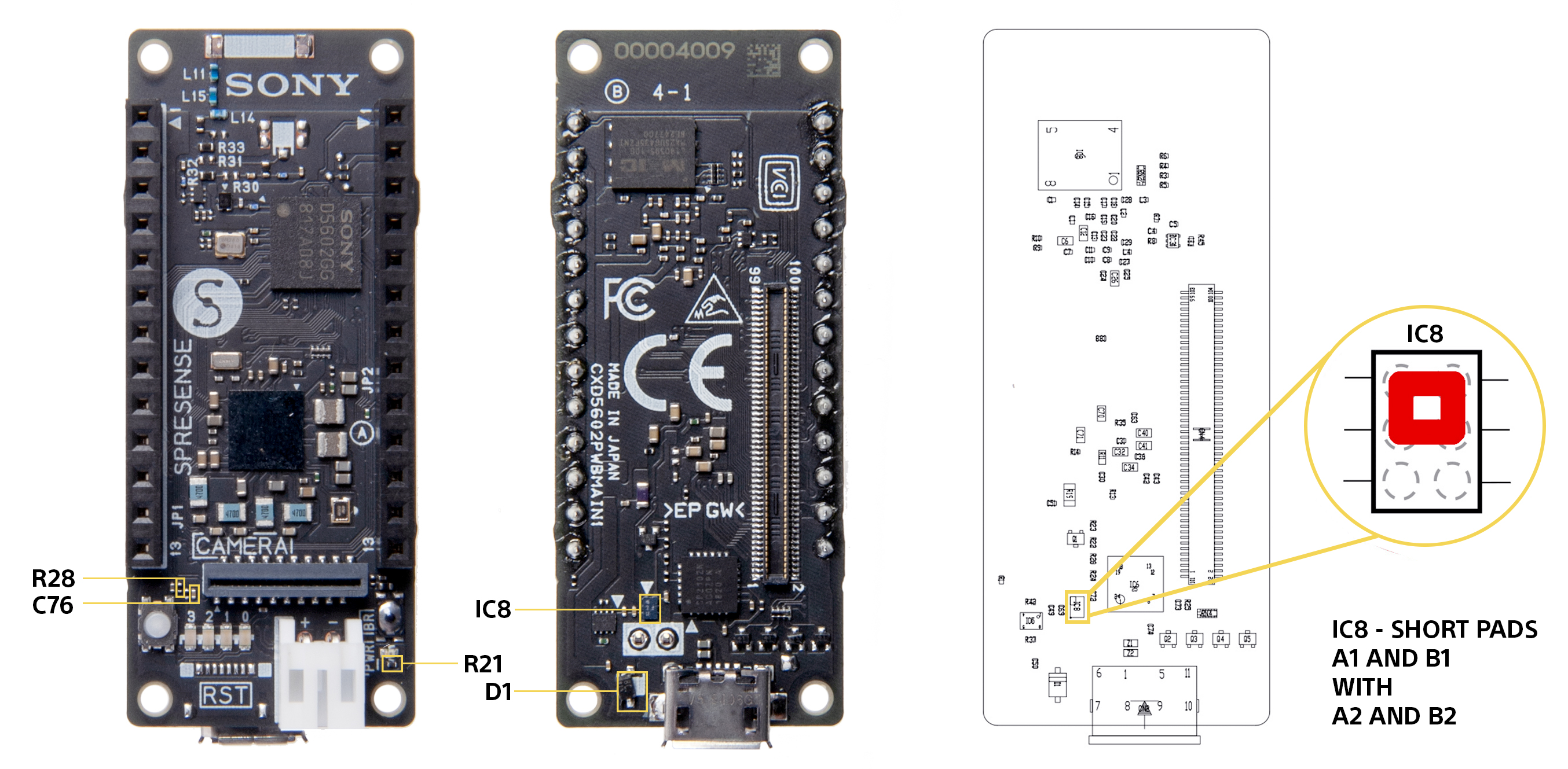
After these modifications the Spresense mainboard cannot be powered via USB anymore so it should only be powered via the battery connector CN1. Beware of the voltage limitations on the CN1 connector.
1.17.2. Software
    /* Sketch to achieve ~6µA during deep sleep */

    #include <LowPower.h>
    #include <stdlib.h>
    #include <RTC.h>

    #define DEEPSLEEP_TIME 5
    #define AWAKE_TIME 5*1000

    void setup() {
        LowPower.clockMode(CLOCK_MODE_32MHz);
        RTC.begin();
        Serial2.begin(115200);
    }

    void loop() {
        ledOn(LED1);

        Serial2.print("Awake for ");
        Serial2.println(AWAKE_TIME/1000);

        delay(AWAKE_TIME);
        ledOff(LED1);

        Serial2.print("Sleep for ");
        Serial2.println(DEEPSLEEP_TIME);

        LowPower.deepSleep(DEEPSLEEP_TIME);
    }
1.18. How to use microphones
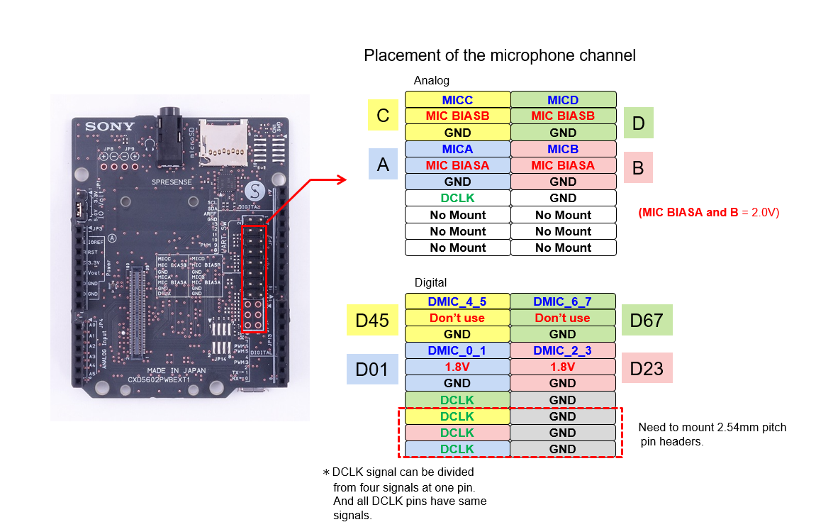
The Spresense extension board can be connected to maximum 4 analog or 8 digital microphones via JP10’s 2.54mm pitch header.
The Spresense extension board is set to analog microphone mode when shipped.
To use digital microphones, the extension board needs to be configured by soldering. This configuration requires soldering of very small components and should only be attempted by people with appropriate skills and equipment.
| Modifying the Spresense boards will void the warranty. Please do it at your own risk. |
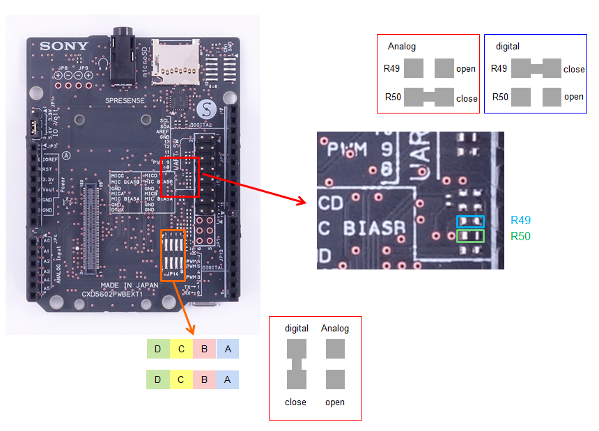
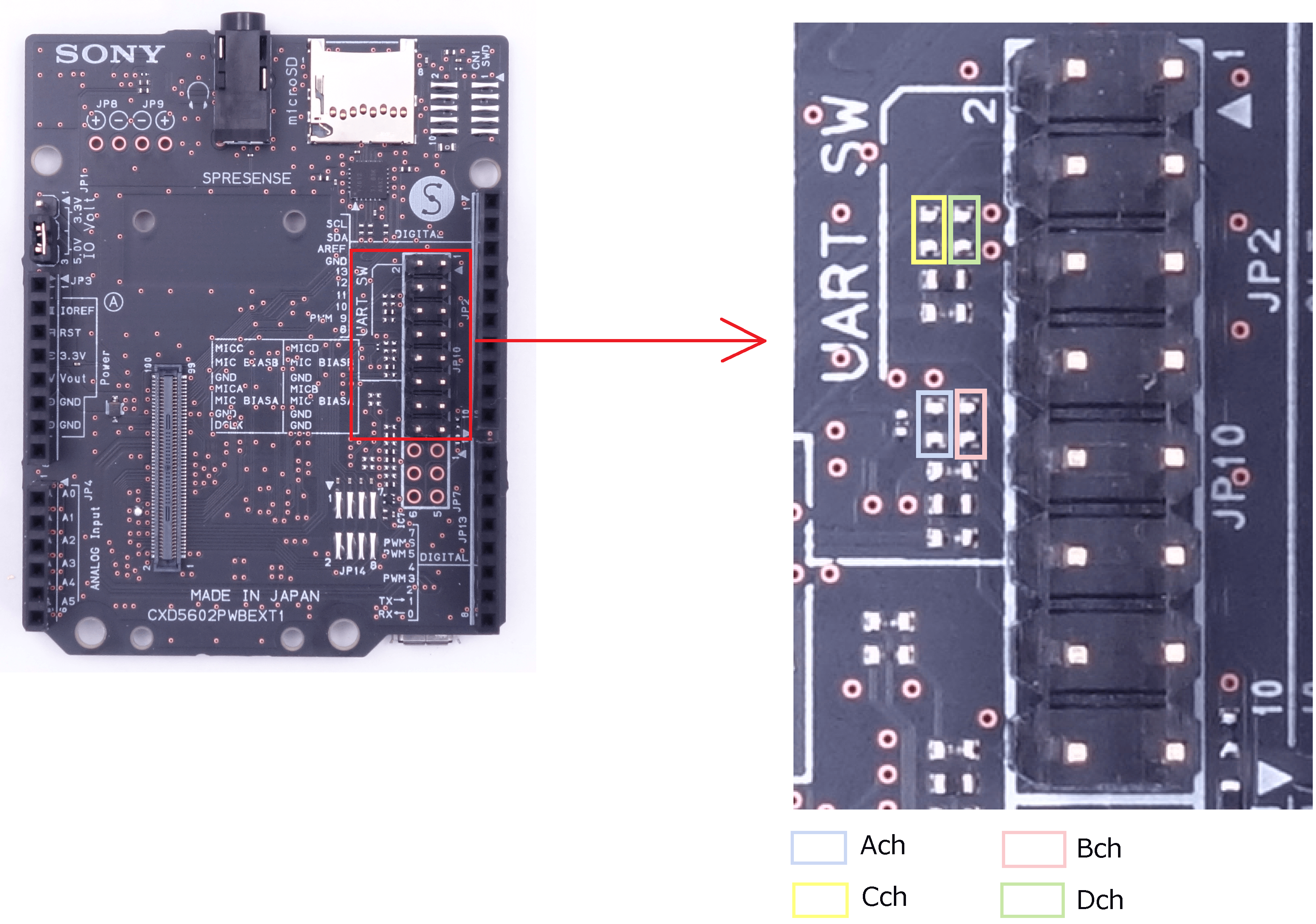
1.18.1. Placement of the microphone channel
The image below in this section will show where the microphone pin header (JP10 in the schematic) is located on the extension board.
In this image, the groups of A,B,C and D are analog microphone channels, and the groups of D01, D23, D45 and D67 with same color are digital microphone channels.
If the analog microphone or digital microphone input settings are set separately for each channel, sufficient input sound quality performance may not be obtained. It is recommended to set all channels to analog microphone or digital microphone input.
1.18.2. How to change microphone mode from analog to digital
It is necessary to make modifications to the hardware to change the microphone mode from analog to digital.
-
Remove R50 and mount 0 Ω to R49 (or short with a jumper wire etc).
-
To enable digital a microphone channel pair, an upper and a lower pad pair on JP14 have to be shorted. Jumper wire can be soldered to connect the pads or just solder the pads together.
The best way to change microphone mode is to use 1.27mm pitch short jumpers as stated below.
-
1.27mm pitch 8pin headers (surface mount type) can be mounted on the solder pads on JP14.
This enables to select the digital microphone mode by using a jumper.
| Vendor | Pin header | Short jumper |
|---|---|---|
Samtec |
FTS-104-01-L-DV-TR |
|
HARWIN |
M50-1900005 |
|
HIROSUGI |
PSM-720153-04 |
JS-7 |
JC ELECTRONICS |
IKHSM28-D08G-H1.5 |
HSH-JB-G |
1.18.3. How to connect analog microphones
1.18.3.1. Dynamic microphones
The microphone interface provides 4 analog microphone inputs, MICA, MICB, MICC and MICD. These terminals are AC-coupled by capacitors. It is important to use the GND on JP10 for the lowest noise operation.
1.18.3.2. Electret Microphones
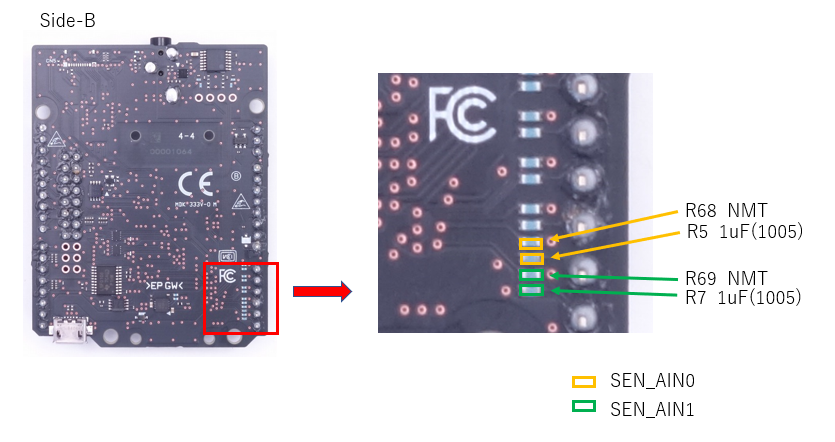
2 wire electret condenser based microphones need to be biased with a 2.0V bias voltage on the input lines. To activate the bias voltage on the input line it is necessary to mount load resistors (RL) (size 1005 metric or 0402 imperial) on the extension board.
The table below will show what resistor that will activate the bias voltage for each channel on JP10.
The load resistor value is recommended for each microphone, please check the data sheet of the microphone used. The output impedance of the microphone is almost the value of the load resistor.
| Microphone channel | Resistor ref to mount |
|---|---|
A |
R51 |
B |
R52 |
C |
R47 |
D |
R48 |
The following is an example of an electret microphone that can be used. The recommended microphone load resistor for the following microphones is 2.2kΩ.
| Vendor | Model |
|---|---|
CUI |
CMC-5044PF-A |
PUI |
POM-3535P-3-R |
Soberton |
EM-6022P |
1.18.3.3. Analog MEMS Microphones
For analog MEMS microphones the bias pins on JP10 provide power to the MEMS microphone, connect the bias pin of JP10 to the MEMS microphones power supply pin.
| Vendor | Model |
|---|---|
Knowles |
SPU0414HR5H-SB |
Knowles |
SPH1642HT5H-1 |
1.18.4. How to connect digital microphones
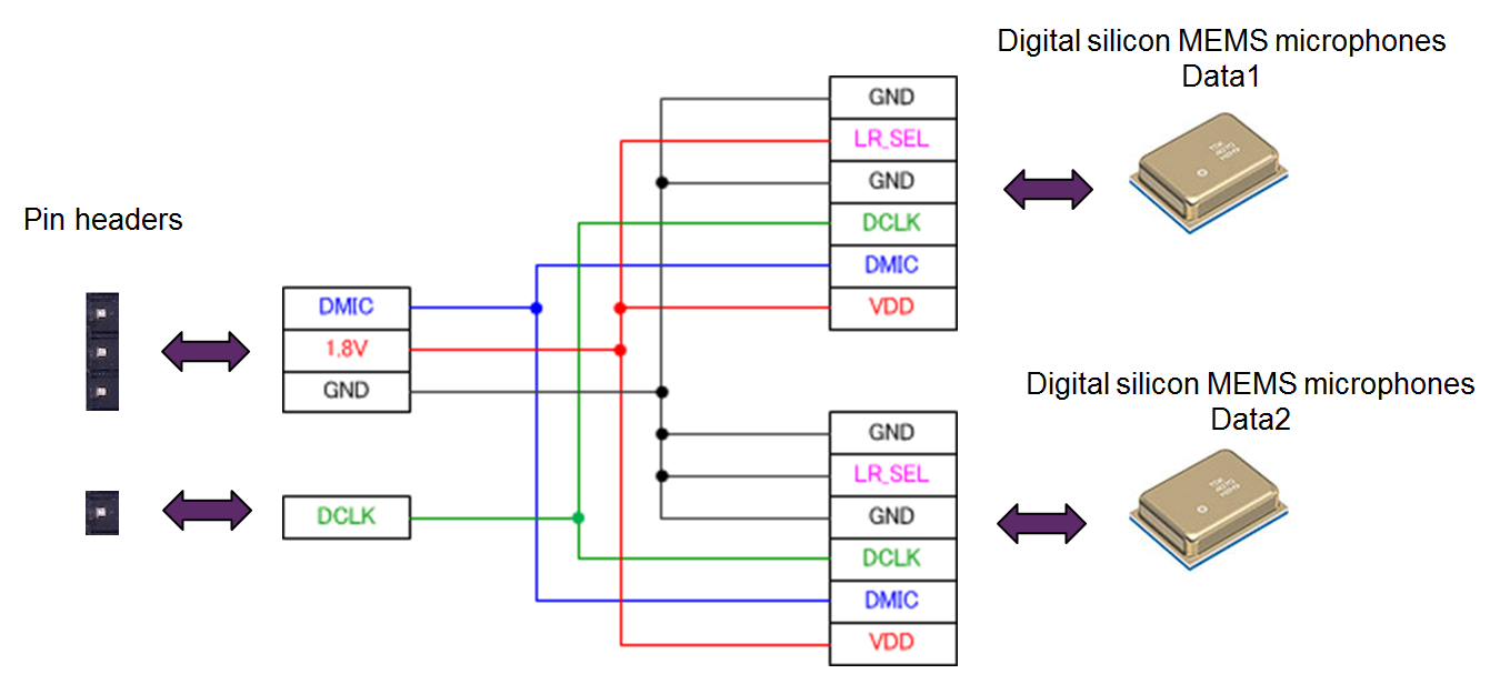
The following way is the recommended way of connecting digital microphones to the extension board. Two digital silicon MEMS microphones can be connected using 4 pins on the JP10 pin header per microphone pair.
It is necessary to select what side each microphone in a pair is, this is done by setting the left/right select signal (LR_SEL) to LOW on one microphone and to HIGH on the other microphone. Each microphone has to connect four more pins, DMIC for data, DCLK for clock, GND to ground and VDD to 1.8V power supply.
It is possible to use the 1.8V from the MIC_BIAS pin on the extension board terminals of the A and B channel (C and D channel MIC_BIAS cannot be used).
| Vendor | Model |
|---|---|
Knowles |
SPH0641LU4H-1 |
Knowles |
SPM0423HD4H-WB |
Infineon |
IM69D130 |
1.19. How to use speakers
CXD5247 on Spresense main board has an on-chip Class-D stereo amplifier that can drive a stereo pair of speakers.
This section will describe how to configure the Spresense boards to enable the speaker output when using the main board together with the extension board.
The Class-D stereo amplifier can produce up to 400mW into 8Ω impedance speakers.
- Speakers with main board alone
-
It is not possible to use speakers directly with the main board without using an external voltage source and an external circuit with similar function as the audio circuit on the extension board.
It is necessary to supply low noise 3.3V from an external source to Pin 1 and Pin 3 on the board to board connector (CN4 on the main board) to power the Class-D amplifier. Supply current must be sufficient to drive the attached speakers - Speakers with main board and extension board
-
The extension board has a 3.3V power supply designed to supply the Class-D amplifier. The default configuration of the main board is to output audio to the headphone jack on the extension board.
To use speakers it is necessary to replace small chip components on the main board and attach speaker cords to the extension board.
This modification requires soldering of very small components and should only be attempted by people with appropriate skills and equipment.
| Modifying the Spresense boards will void the warranty. Please do it at your own risk. |
1.19.1. Main board modifications to support speakers
The modifications are needed to filter the output from the Class-D amplifier of the CXD5247 when used to drive speakers.
Replace the following components:
-
R15, 16, 17, 18 → 15uH/220mA(2012) [orange frame in the picture below]
replace to inductors.
recommend to use BRL2012T150M made by Taiyo Yuden. -
C45, 46, 47, 48 → 0.47uF(1005) [green frame in the picture below]
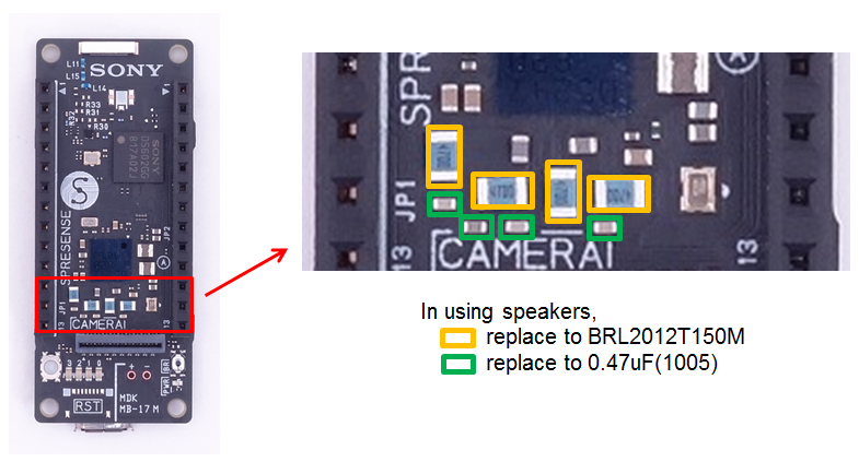
| Do not use the headphones with the extension board after doing this modification. |
1.19.2. Extension board modifications to support speakers
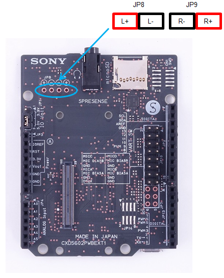
Mount 2.54mm pitch pin header on JP8 and JP9 to connect speakers (or solder speaker cords directly to the board).
| The Spresense board is designed to drive speakers differentially. The left and right speaker negative connections should not be connected together. |
1.20. How to use JTAG Debugger
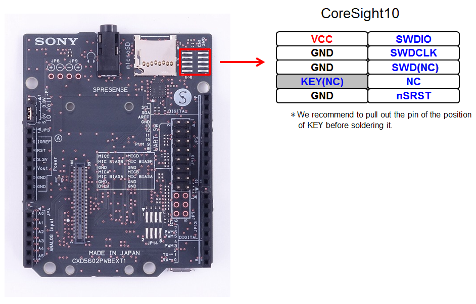
You can use a JTAG/SWD debugger for Cortex-M series ARM microcontrollers by using the CoreSight 10 connector on the Spresense extension board. Interface voltage is 3.3V.
The Spresense CoreSight 10 connector is intended for serial wire debug (SWD) only. It does not support JTAG, because the SWD pin (can be called TDO/SWO), which is used also for JTAG TDO, is not connected on the extension board.
The extension board comes with a CoreSight 10 footprint but with no pin header mounted. To mount a pin header it is necessary to solder the pin header onto the board. This modification requires soldering of small components and should only be attempted by people with appropriate skills and equipment.
| Modifying the Spresense boards will void the warranty. Please do it at your own risk. |
To use the SWD function, you have to mount a connector (1.27mm pitch 10 pin header) for CoreSight 10 at CN1 on the Spresense extension board.
The connector hole on the position of KEY on the cable side of the CoreSight 10 connector can be blocked. So it is recommended to remove the pin on position KEY from the pin header before it is soldered onto the extension board. See picture below.
| Vendor | Pin Header |
|---|---|
Samtec |
FTS-105-01-L-DV-TR |
HARWIN |
M50-3600542 |
HIROSUGI |
PSM-720153-05 |
JC ELECTRONICS |
IKHSM28-D10G-H1.5 |
1.21. How to use GNSS
1.21.1. About On-board chip antenna for GNSS
The Spresense is equipped with a chip antenna for GNSS on the main board, and positioning is possible in that state.
The characteristics of the onboard antenna are shown below. The characteristics of on board GNSS chip antenna (pdf)
1.21.2. How to use the external antenna for GNSS
The Spresense can also be used to connect an external uFL connection type antenna to the main board for higher performance positioning.
If you connect an external antenna to the uFL connector, higher-performance positional measurement is possible. To do this you have to solder a uFL connector on the main board. This modification requires soldering of very small components and should only be attempted by people with appropriate skills and equipment.
| Modifying the Spresense hardware by performing soldering work as described here will void the product warranty. Please proceed at your own risk. |
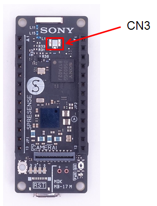
The following steps will describe the necessary work needed to fit an uFL connector to be able to use an external GNSS antenna.
-
Mount the uFL connector on CN3, see the picture below.
| Vendor | Model |
|---|---|
Hirose Electric |
U.FL-R-SMT-1 |
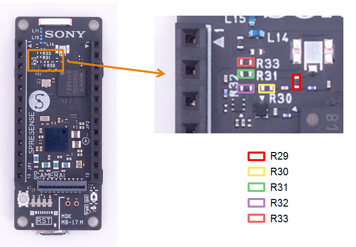
-
Depending on the type of the antenna you plan to use, the resistor chips have to be changed on the main board as shown in the table below.
In the table below, "OPEN" stands for the status that a part is not mounted in the applicable location, and "CLOSE" stands for the status that it is short-circuited with 0 Ω resister or a wire.
| Antenna | R29 | R31 | R33 | R30 | R32 | Note |
|---|---|---|---|---|---|---|
chip (on board) |
CLOSE |
OPEN |
CLOSE |
OPEN |
CLOSE |
default |
passive (external) |
OPEN |
CLOSE |
OPEN |
OPEN |
CLOSE |
|
active (external) |
CLOSE |
OPEN |
CLOSE |
CLOSE |
OPEN |
3.3V supplied to antenna |
1.22. Spresense Add-on board / extension board / case design
1.22.1. Spresense HW design material
Spresense publishes various hardware design materials for all boards that are useful for designing Add-on boards, extension boards, and cases.
-
Schematics
-
Bill of Materials
-
Dimensions
-
Parts layout
-
2D CAD DATA(DXF)
-
3D CAD DATA(STEP)
In addition, the connector pin list and GNSS onboard chip antenna characteristics are also disclosed.
These are collectively published in Hardware Design Documents.
1.22.2. Precautions for board dimensions when designing Spresense Add-on boards
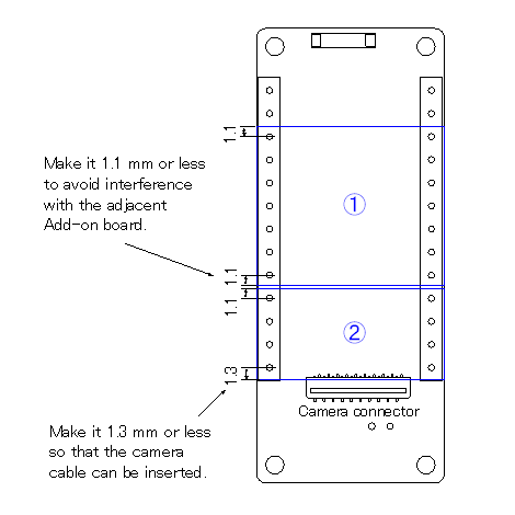
In order to mount multiple Spresense Add-on boards in the pin sockets on the main board, it is necessary to pay attention to the board dimensions.
The figure below shows the points to be noted when designing the board dimensions, taking as an example the case of designing two Add-on boards (1) and (2).
1.22.3. Precautions when using the onboard chip antenna for GNSS on the Spresense main board
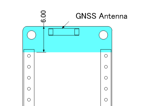
When positioning GNSS using a newly designed board and the onboard chip antenna for GNSS on the Spresense main board, pay attention to the design around the antenna in order to ensure the reception sensitivity of the antenna. .
When designing an Add-on board or extension board that overlaps the light blue colored part in the figure below, do not place metal-containing parts or copper foil patterns on the corresponding part of each board.
2. Differences between Spresense and Arduino Uno
The pin header on the Spresense extension board is compatible with Arduino Uno pins. Spresense and Arduino Uno are the same size. The following table lists the functional differences:
| Function | Spresense | Arduino Uno |
|---|---|---|
Supply voltage on header |
VOUT pin: 5V can be connected to the pin to power the boards |
VIN pin: 7 to 12V. |
Digital IO Voltage |
3.3V or 5V. |
Fixed 5V only. |
GPIO As output |
Extension board uses level shifters with 1KΩ pull-up resistors on all GPIO. Pull-ups are not compatible with some existing shield designs. GPIO pin’s typical sink current is several mA at 5V IO voltage. [1] |
Directly driven from the ATmega328 MPU and can deliver up to 40mA per pin. |
GPIO As input |
Extension board uses level shifters with 1KΩ pull-up resistors on all GPIO. Pull-up resistors are not compatible with all shield designs. [1] |
The ATmega328 MPU has a high-input impedance. |
Analog pins A0-A5 as GPIO |
Can only be used as analog in. |
Can be used as analog in pins or as GPIO. |
Analog pins A0-A5 impedance |
A0 to A3 72k Ohms, A4 and A5 37k Ohms |
100M Ohm |
Analog pins A0-A5 reference voltage |
Fixed 5V ADC reference. [2] |
Settable sources as ADC reference. |
VREF pin |
Output digital I/O voltage reference. |
Input reference for ADC. |
USB ports |
Two ports: main board (Serial monitor) and extension board (Mass Storage). |
One. |
Serial communication |
Main board USB is addressed as UART |
UART shared with DO0 DO1 addressed as |
SPI pin |
Master mode only. |
Master/Slave both mode supported. |
DO0 DO1 serial communication |
UART2 addressed as |
UART shared with USB addressed as |
| [1] Digital Input/Output Pins: 1.8 V of CXD5602 is converted to 3.3 V or 5 V via the level shifter on the extension board. It is connected to the pin socket via a pull-up resistor, which may cause problems depending on the shield and device connected. |
| [2] Analog Input Pins: Since the analog input range of CXD5602 is 0.7 V, resistance voltage division is adopted to lower the voltage from 5 V to 0.7 V. Since this method may cause problems depending on the connected device, when using the AIN terminal on the extension board, pay attention to the output impedance of the connected device. |
3. Spresense Hardware comparison
To better introduce Spresense board’s features, it is compared with Arduino Uno and Raspberry PI (model 3B), which are known to many developers.
3.1. Processor and OS
Feature |
Arduino Uno |
Spresense |
Raspberry Pi 3B |
Processor type |
AVR |
ARM M4F |
ARM A53 |
Bits |
8 |
32 |
64 |
Number of cores |
1 |
6 |
4 |
Clock speed |
16 MHz |
156 MHz |
1.2 GHz |
Operating system |
None |
NuttX |
Linux |
Boot time |
0 |
<1 second |
~20 Seconds |
Spresense has a processor that is far more powerful than Arduino. This allows it to be used for applications which are computationally intensive, but it does not match the performance of the Raspberry Pi.
The Spresense has the advantage of an operating system while still having a typical boot time of under 1 second.
3.2. Memory
Feature |
Arduino Uno |
Spresense |
Raspberry Pi 3B |
RAM |
0.002MB |
1.5 MB |
1000MB |
FLASH |
0.032MB |
8 MB |
None |
SD Card |
Shield |
On-Board, optional |
On-Board, essential |
eMMC |
None |
Shield |
None |
EEPROM |
0.001MB |
Use Flash |
Use microSD card |
Arduino has a small memory size, which is a limiting factor for complex programs. Even the Arduino Mega only has 256k flash and 8k SRAM. The Raspberry Pi has much larger memory, but relies on having a microSD card instead of on board Flash.
Spresense fits between these two extremes. It has the advantage of 8MB on board Flash memory and 1.5MB RAM. It also has support for microSD card, without the need for a shield, when larger memory is required.
Spresense doesn’t have EEPROM, but EEPROM library emulates EEPROM using flash memory. If you want to handle persistent data, you can use the EEPROM library or the microSD card on the extension board.
3.3. Power
Feature |
Arduino Uno |
Spresense |
Raspberry Pi 3B |
Voltage |
5V or 6-20V |
5V or LiPo(3.7V) |
5V |
Typical Operating Power |
50 mW |
100mW + low power modes |
2400mW |
The CXD5602 and the CXD5247 were designed for use in wearable products powered by a single LiPo battery. The battery charge function is not available on the Spresense boards. Spresense main and extension boards are designed to be powered from 5V, for example directly from a USB port.
Spresense has been optimized to provide a high processing capability while consuming little power. It supports multiple low power modes allowing long battery life from smaller batteries than Raspberry Pi, which make it great for battery or renewable powered IoT applications.
3.4. Audio
Feature |
Arduino Uno |
Spresense |
Raspberry Pi 3B |
Quality |
Shield |
High |
Low |
Microphones |
Shield |
up to 8 microphone |
Stereo |
Speakers |
Shield |
Stereo |
Stereo |
The CXD5602 and the CXD5247 have been designed as a chipset to support high quality audio recording and playback. The CXD5247 includes a high quality ADC for up to 4 analog inputs or up to 8 digital microphone. The CXD5602 includes a dedicated DSP for Audio processing and stereo audio output.
3.5. GNSS and Real Time clock
Feature |
Arduino Uno |
Spresense |
Raspberry Pi 3B |
GNSS |
Shield |
GPS & GLONASS |
Shield |
Time |
Shield |
RTC |
Shield |
The Spresense has an ultra low power GNSS receiver. This allows precise positioning for applications such as tracking devices and drones. It also includes a real time clock which is great for data logging. Arduino and Raspberry Pi need shields to implement these functions.
3.6. Digital IO
Feature |
Arduino Uno |
Spresense |
Raspberry Pi 3B |
IO Pins |
14 |
29 + 4 LED |
27 |
IO voltage |
5V |
5V/3.3V/1.8V |
3.3V |
UART |
1 |
2 |
2 |
SPI |
1 |
1 (3.3/5V) +1 (1.8V) |
1 |
I2C |
1 |
1 (3.3/5V) +1 (1.8V/camera) |
2 |
PWM |
6 |
4 |
1 |
The Spresense has a wide range of digital IO pins and hardware UART, I2C, SPI and PWM channels. It supports IO voltages of 5V, 3.3V and 1.8V which make it easy to connect to many devices. It has 4 on board LEDs instead of using available GPIO pins for LEDs. Spresense provides even more IO capability for custom shields with the 100 B2B connector.
3.7. Analog to digital converter
Feature |
Arduino Uno |
Spresense |
Raspberry Pi 3B |
Channels |
6 |
6 |
None |
Bits |
10 |
10 |
None |
Fastest rate |
~10 kHz |
500 kSPS |
None |
Spresense, like Arduino, has 6 analog input channels, but unlike Arduino these are dedicated pins which do not reduce the usable number of digital IO. Two of the Spresense analog channels are high speed with anti-aliasing. This is in addition to 4 microphone ADCs on the CXD5247.
3.8. Connectivity
Feature |
Arduino Uno |
Spresense |
Raspberry Pi 3B |
USB |
1 device |
2 device |
4 host |
Camera |
Shield |
5M Pixel |
8M Pixel |
Video display |
None |
SPI up to 360x240 Pixel |
HDMI, DSI |
WiFi |
Shield |
Shield |
802.11n |
Bluetooth |
Shield |
Shield |
4.1 Classic, Low Energy |
Ethernet |
Shield |
Shield |
10/100 |
Cellular |
Shield |
Shield |
Shield |
Spresense like Raspberry Pi is designed with direct connection to camera. It can support HD resolution, still images and low resolution video for a viewfinder. Like Arduino, any wireless communication requires a shield.